
The modern digital world runs on semiconductors. From smartphones and laptops to medical devices and advanced automotive systems, semiconductors power nearly every piece of technology people use daily. However, few people understand where semiconductor materials actually begin.
A key starting point in the semiconductor manufacturing process is the ingot. Understanding what an ingot in semiconductor manufacturing is helps explain how raw silicon eventually becomes advanced microchips and integrated circuits.
Companies involved in precision cutting, wafer preparation, and semiconductor material processing rely on specialized tools and expertise to transform ingots into functional semiconductor components. Manufacturers such as Ukam Industrial Superhard Tools support this process by supplying advanced diamond tools designed for high-precision semiconductor machining.
This article explains the role of semiconductor ingots, how they are produced, and how they move through the manufacturing journey from crystal growth to integrated circuits.
Understanding the Semiconductor Manufacturing Process
The semiconductor manufacturing process is a complex sequence of highly controlled steps that transform raw materials into functional electronic components.
It typically includes:
Silicon purification
Crystal growth
Ingot formation
Wafer slicing
Wafer polishing and preparation
Integrated circuit fabrication
Among these stages, the ingot formation step is critical because it creates the single-crystal silicon structure required for high-performance semiconductor devices.
Without high-quality ingots, the rest of the semiconductor fabrication process cannot achieve the required precision, reliability, and electrical performance.
What Is an Ingot in Semiconductor Manufacturing?
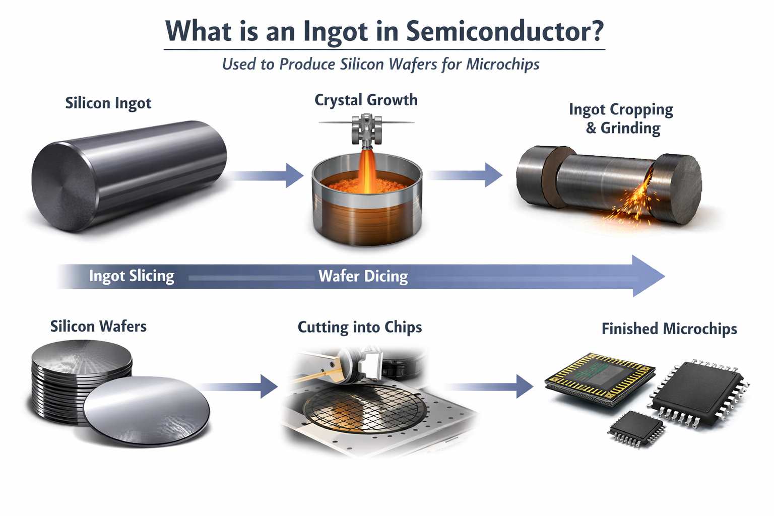
An ingot in semiconductor manufacturing is a large, cylindrical block of ultra-pure single-crystal silicon that serves as the starting material for producing semiconductor wafers.
The ingot acts as the parent structure from which thin silicon wafers are sliced. These wafers later become the foundation for integrated circuits used in electronic devices.
Key Characteristics of Semiconductor Ingots
Semiconductor ingots must meet extremely strict material standards, including:
Ultra-high purity silicon
Single crystal structure
Precise diameter and orientation
Minimal crystal defects
These properties ensure that semiconductor wafers derived from the ingot can support the microscopic circuitry required in modern electronics.
Why Ingot Quality Matters in Semiconductor Production
The entire semiconductor manufacturing process depends on the quality of the ingot.
Even small structural imperfections can affect:
Electrical conductivity
Chip performance
Device reliability
Manufacturing yield
For this reason, semiconductor manufacturers invest heavily in crystal growth technology, precision slicing equipment, and advanced machining tools to maintain consistent ingot quality.
Precision diamond tools from companies such as Ukam Industrial Superhard Tools are often used during ingot slicing and wafer preparation to ensure extremely accurate cutting with minimal material loss.
How Semiconductor Ingots Are Made
Semiconductor ingots are produced through specialized crystal growth processes that convert purified silicon into a single crystal structure.
1. Silicon Purification
The process begins with silicon extracted from quartz. This silicon undergoes multiple purification stages until it reaches electronic-grade purity suitable for semiconductor fabrication.
Impurities must be reduced to extremely low levels to ensure proper electrical performance in the final chips.
2. Crystal Growth
Once purified, the silicon is melted inside a high-temperature furnace. A small seed crystal is then introduced into the molten silicon.
As the crystal slowly rotates and is pulled upward, the molten silicon solidifies around the seed, forming a single continuous crystal structure.
This method ensures the crystal lattice remains consistent throughout the ingot.
3. Ingot Formation
As the crystal continues to grow, it forms a long cylindrical structure called an ingot.
These ingots can reach several feet in length and weigh hundreds of kilograms depending on the semiconductor manufacturing requirements.
At this stage, the ingot is carefully cooled and inspected to verify structural consistency and crystal alignment.
From Semiconductor Ingot to Silicon Wafer
Once the ingot is formed, it undergoes several machining steps before becoming usable semiconductor wafers.
Ingot Shaping
The cylindrical ingot is first ground to achieve a precise diameter. Flat edges or notches are sometimes added to indicate crystal orientation for later fabrication steps.
Wafer Slicing
Next, the ingot is sliced into extremely thin circular wafers using diamond wire saws or precision cutting tools.
This step requires exceptional accuracy because:
Wafer thickness must be extremely consistent
Material waste must be minimized
Surface damage must be avoided
Diamond cutting technologies from Ukam Industrial Superhard Tools are designed specifically for this level of precision in semiconductor material processing.
Wafer Polishing and Preparation
After slicing, wafers undergo multiple polishing stages to achieve a mirror-smooth surface.
This polishing process removes microscopic damage from cutting and prepares the wafer surface for integrated circuit fabrication.
How Ingots Become Integrated Circuits
After wafers are prepared, they move into semiconductor fabrication facilities where complex electronic circuits are built onto their surfaces.
This stage includes processes such as:
Photolithography
Ion implantation
Etching
Thin film deposition
Through these processes, billions of microscopic transistors are created on a single wafer, forming the integrated circuits that power modern electronics.
The journey from silicon ingot to integrated circuit is one of the most advanced manufacturing processes in the world.
Tools Used in Semiconductor Ingot Processing
Working with semiconductor materials requires specialized tools that can cut extremely hard materials while maintaining microscopic precision.
Key tools used during ingot processing include:
Diamond wire saws
Precision diamond blades
Diamond core drills
Wafer slicing tools
Surface grinding tools
These tools must deliver extremely clean cuts with minimal vibration or heat damage.
Ukam Industrial Superhard Tools, a manufacturer based in the USA, develops advanced diamond tooling solutions used across semiconductor manufacturing applications, including ingot slicing and wafer preparation.
Challenges in Semiconductor Ingot Processing
Producing semiconductor ingots and converting them into wafers involves several technical challenges.
Maintaining Crystal Integrity
The single crystal structure must remain consistent across the entire ingot. Any disruption can impact wafer performance.
Minimizing Material Waste
Silicon materials are expensive to produce. Efficient slicing methods help reduce kerf loss and maximize wafer yield.
Achieving Precision Cutting
Wafer thickness tolerances are extremely tight, requiring high-performance diamond cutting technologies.
Why Advanced Tooling Matters in the Semiconductor Industry
As semiconductor technology continues to advance, the demand for ultra-thin wafers and larger wafer diameters continues to grow.
This increases the need for:
Higher precision cutting tools
Improved surface finishing technologies
More efficient wafer processing equipment
Manufacturers like Ukam Industrial Superhard Tools contribute to this ecosystem by developing diamond cutting solutions designed for semiconductor materials, helping fabrication facilities achieve the accuracy and efficiency required for modern chip production.
The Growing Importance of Semiconductor Manufacturing
Semiconductors are now central to nearly every industry, including:
Consumer electronics
Automotive technology
Telecommunications
Medical equipment
Aerospace systems
Because of this demand, the semiconductor manufacturing process continues to evolve, pushing advancements in crystal growth, wafer slicing, and precision machining technologies.
The ingot remains the essential starting point in this entire manufacturing chain.
Final Thoughts
Understanding what an ingot in semiconductor manufacturing is helps reveal the foundation of modern electronics. The ingot represents the transition from purified silicon to structured semiconductor material capable of supporting advanced microchips.
From crystal growth to wafer slicing and integrated circuit fabrication, every stage of the semiconductor manufacturing process depends on precision engineering and advanced material processing.
With the support of specialized tooling providers such as Ukam Industrial Superhard Tools in the USA, semiconductor manufacturers can achieve the accuracy, efficiency, and reliability required to produce the technologies that power today’s digital world.
Frequently Asked Questions
What is an ingot in semiconductor manufacturing?
An ingot in semiconductor manufacturing is a large single-crystal cylinder of ultra-pure silicon. It serves as the base material from which thin semiconductor wafers are sliced for electronic device production.
Why are semiconductor ingots important?
Semiconductor ingots form the foundation of the entire semiconductor manufacturing process. High-quality ingots ensure that wafers have the structural consistency needed for reliable electronic circuits.
How are semiconductor ingots produced?
Semiconductor ingots are produced by melting purified silicon and slowly growing a single crystal using specialized crystal growth techniques. The crystal is pulled upward from molten silicon to form a cylindrical ingot.
What happens after the ingot is formed?
After formation, the ingot is shaped, sliced into thin wafers, polished, and then used in semiconductor fabrication processes that create integrated circuits.
What tools are used to process semiconductor ingots?
Processing semiconductor ingots requires precision diamond tools such as diamond wire saws, wafer slicing blades, and grinding equipment. These tools enable accurate cutting while protecting the material structure.